Texas InstrumentsUnited States

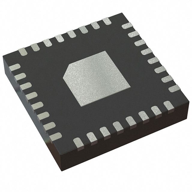
IC STEREO AUDIO CODEC 1.8V 32QFN
TLV320AIC3204IRHBR is an ultra-low power stereo audio codec with 100dB SNR DAC and 93dB SNR ADC, in a 5mm x 5mm 32-pin VQFN package, featuring integrated PLL and LDO for portable audio applications.Checked against the datasheet
All alternatives
View full reportTechnical parameters
Datasheet-verified parameters
21 items| Parameter | Value and test conditions | Source |
|---|---|---|
| Package | VQFN (32), 5.00 mm x 5.00 mm | |
| Operating Temperature Range | -40 to 85 °C | |
| RoHS | Yes | |
| AVDD Power Supply Voltage Range | Min 1.5 V, Nom 1.8 V, Max 1.95 V (Referenced to AVSS) | |
| DVDD Power Supply Voltage Range | Min 1.26 V, Nom 1.8 V, Max 1.95 V (Referenced to DVSS) | |
| IOVDD Power Supply Voltage Range | Min 1.1 V, Max 3.6 V (Referenced to IOVSS) |
All parameters (18)
| Power | |
|---|---|
| Voltage - Supply, Analog | 1.5V ~ 1.95V |
| Voltage - Supply, Digital | 1.26V ~ 1.95V |
| AC and DC characteristics | |
| Resolution (Bits) | 32 b |
| Environment and package | |
| Mounting Type | Surface Mount |
| Operating Temperature | -40°C~85°C |
| Package | Tape & Reel (TR); Cut Tape (CT); Digi-Reel® |
| Package / Case | 32-VFQFN Exposed Pad |
| Supplier Device Package | 32-VQFN (5x5) |
| Other | |
| Base Product Number | TLV320 |
| Data Interface | Serial |
| Dynamic Range, ADCs / DACs (db) Typ | 92 / 100 |
| Mfr | Texas Instruments |
| Number of ADCs / DACs | 2 / 2 |
| Product Status | Active |
| Series | - |
| Sigma Delta | Yes |
| S/N Ratio, ADCs / DACs (db) Typ | 93 / 100 |
| Type | Stereo Audio |
Pinout and package
PackageVQFN (32), 5.00 mm x 5.00 mm
| Pin | Name | Function | Source |
|---|---|---|---|
| 1 | MCLK | (Master Clock Input) | |
| 2 | BCLK | (Bit Clock Input) | |
| 3 | WCLK | (Word Clock Input) | |
| 4 | DIN/MFP1 | (Digital Audio Input/Multipurpose Function Pin 1) | |
| 5 | DOUT/MFP2 | (Digital Audio Output/Multipurpose Function Pin 2) | |
| 6 | IOV_DD | (I/O Power Supply Positive) | |
| 7 | IOV_SS | (I/O Power Supply Negative) | |
| 8 | SCLK/MFP3 | (SPI Clock/Multipurpose Function Pin 3) | |
| 9 | GPIO/MFP5 | (General Purpose I/O/Multipurpose Function Pin 5) | |
| 10 | SCL/SS | (I2C Clock/SPI Slave Select) | |
| 11 | RESET | (Reset) | |
| 12 | SDA/MOSI | (I2C Data/SPI Master Out Slave In) | |
| 13 | LDO_SELECT | (LDO Select) | |
| 14 | MISO/MFP4 | (SPI Master In Slave Out/Multipurpose Function Pin 4) | |
| 15 | DV_DD | (Digital Power Supply Positive) | |
| 16 | SPI_SELECT | (SPI Select) | |
| 17 | DV_SS | (Digital Power Supply Negative) | |
| 18 | IN1_L | (Analog Input 1 Left) | |
| 19 | HPR | (Headphone Output Right) | |
| 20 | IN1_R | (Analog Input 1 Right) | |
| 21 | LDOIN | (LDO Input) | |
| 22 | IN2_L | (Analog Input 2 Left) | |
| 23 | HPL | (Headphone Output Left) | |
| 24 | IN2_R | (Analog Input 2 Right) | |
| 25 | AV_DD | (Analog Power Supply Positive) | |
| 26 | LOR | (Line Output Right) | |
| 27 | LOL | (Line Output Left) | |
| 28 | IN3_R | (Analog Input 3 Right) | |
| 29 | IN3_L | (Analog Input 3 Left) | |
| 30 | MICBIAS | (Microphone Bias) | |
| 31 | REF | (Reference Voltage) | |
| 32 | AV_SS | (Analog Power Supply Negative) |
Documents
Datasheet-verified content is extracted by AI from the manufacturer datasheet. Click a page number to view the original.