MaxLinear, Inc.United States
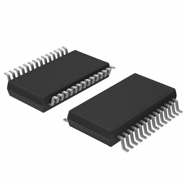
IC TRANSCEIVER FULL 5/3 28SSOP
SP3238EEA-L/TR is a 5-driver/3-receiver RS-232 transceiver operating from 3.0V to 5.5V in a 28-pin SSOP package, featuring AUTO ON-LINE wake-up and EIA/TIA-232-F compliance.Checked against the datasheet
All alternatives
View full report40 alternatives on file. Sign in to view them.
Technical parameters
Key specs
ProtocolRS-232
Drivers/Receivers5
Data rate250 kbpsMin · RL = 3KΩ,CL = 1000pF
Supply voltage3 ~ 5.5 V
Datasheet-verified parameters
25 items| Parameter | Value and test conditions | Source |
|---|---|---|
| Protocol | EIA/TIA-232-F, EIA/TIA-232, EIA/TIA-562, ITU-T V.28/V.24 | |
| Drivers / Receivers | 5 Drivers / 3 Receivers | |
| Data Rate | 250 kbps (Min) @ RL = 3KΩ, CL = 1000pF, one driver switching | |
| Supply Voltage | +3.0V to +5.5V | |
| Package | 28 Pin SSOP | |
| Operating Temperature | -40°C to +85°C |
All parameters (16)
| Power | |
|---|---|
| Voltage - Supply | 3V ~ 5.5V |
| Environment and package | |
| Mounting Type | Surface Mount |
| Operating Temperature | -40°C~85°C |
| Package | Tape & Reel (TR); Cut Tape (CT); Digi-Reel® |
| Package / Case | 28-SSOP (0.209", 5.30mm Width) |
| Supplier Device Package | 28-SSOP |
| Other | |
| Base Product Number | SP3238 |
| Data Rate | 250kbps |
| Duplex | Full |
| Mfr | MaxLinear, Inc. |
| Number of Drivers/Receivers | 5/3 |
| Product Status | Active |
| Protocol | RS232 |
| Receiver Hysteresis | 500 mV |
| Series | - |
| Type | Transceiver |
Pinout and package
Figure 4. SP3238E Pinout Confi…
| Pin | Name | Function | Source |
|---|---|---|---|
| c1+ | Positive terminal of the symmetrical charge-pump capacitor C1 | ||
| c1- | Negative terminal of the symmetrical charge-pump capacitor C1 | ||
| c2+ | Positive terminal of the symmetrical charge-pump capacitor C2 | ||
| c2- | Negative terminal of the symmetrical charge-pump capacitor C2 | ||
| gnd | Ground | ||
| online | Apply logic HIGH to override AUTO ON-LINE circuitry keeping drivers active (SHUTDOWN must also be logic HIGH) | ||
| r1in | RS-232 | receiver input | |
| r1out | TTL/CMOS | receiver output | |
| r2in | RS-232 | receiver input | |
| r2out | TTL/CMOS | receiver output | |
| r3in | RS-232 | receiver input | |
| r3out | TTL/CMOS | receiver output | |
| shutdown | Apply logic LOW to shut down drivers and charge pump. This overrides all AUTO ON-LINE circuitry and ONLINE | ||
| status | TTL/CMOS | Output indicating if a RS-232 signal is present on any receiver input | |
| t1in | TTL/CMOS | driver input | |
| t1out | RS-232 | Driver Output | |
| t2in | TTL/CMOS | driver input | |
| t2out | RS-232 | Driver Output | |
| t3in | TTL/CMOS | driver input | |
| t3out | RS-232 | Driver Output | |
| t4in | TTL/CMOS | driver input | |
| t4out | RS-232 | Driver Output | |
| t5in | TTL/CMOS | driver input | |
| t5out | RS-232 | Driver Output | |
| v+ | Regulated +5.5V output generated by the charge pump | ||
| v- | Regulated -5.5V output generated by the charge pump | ||
| vcc | +3.0V to +5.5V supply voltage |
Documents
Datasheet-verified content is extracted by AI from the manufacturer datasheet. Click a page number to view the original.