Littelfuse Inc.United States
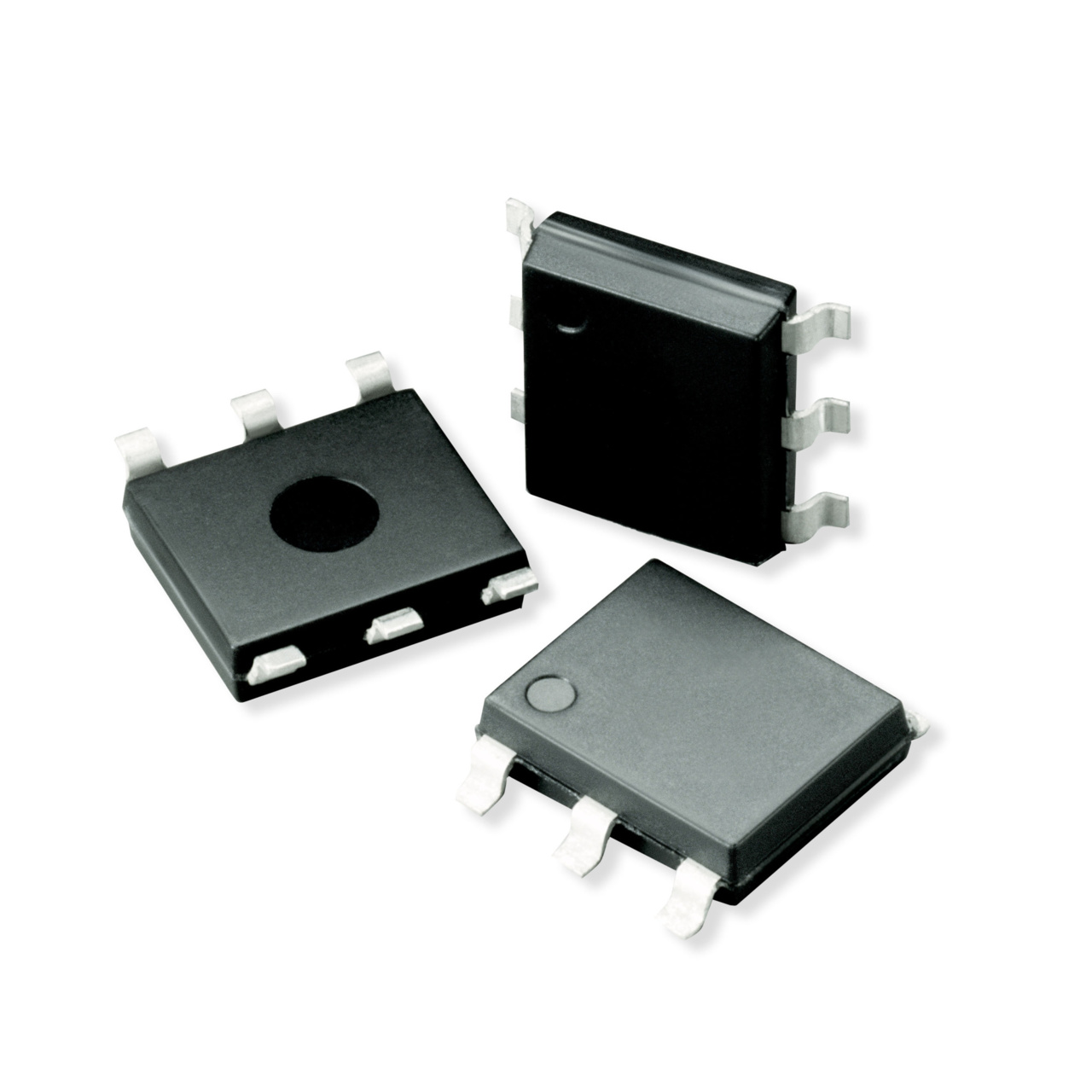
SIDACtor® Uni 4Chp 95V 50A MS013 RoHS
All alternatives
View full reportTechnical parameters
| Power | |
|---|---|
| On-State Voltage Vt | 4 |
| Peak Off-State Voltage Ring to Ground | 95 |
| Peak Off-State Voltage Tip to Ground | 95 |
| Switching Voltage Ring to Ground | 130 |
| Switching Voltage Tip to Ground | 130 |
| Environment and package | |
| Package | MS-013 |
| Other | |
| Circuit Diagram | Quad SLIC |
| Circuit Name | Quad SLIC |
| C O 2V T-R MAX (pF) | 105 |
| C O 2V T-R MIN (pF) | 15 |
| Configuration | Dual Port |
| di/dt (A/µs) | 500 |
| I DRM @ V DRM (µA) | 5 |
| I H (A) | 120 |
| Ipp10x700 | 75 |
| Ipp2x10 | 150 |
| Ipp5x310 | 75 |
| Ipp5x320 | 75 |
| Ipp8x20 | 150 |
| Iscurr | 800 |
| I TSM 60Hz (A) | 20 |
| Max Capacitance Ring to Ground | 160 |
| Max Capacitance Tip to Ground | 160 |
| Min Capacitance Ring to Ground pF | 40 |
| Min Capacitance Tip to Ground | 40 |
| Pins Ring to Ground | 1-2 4-5 |
| Pins Tip to Ground | 3-2 6-5 |
| Pins Tip to Ring | 3-1 6-4 |
| Regulatory Requirements | GR1089 INTER-BUILDING (SERIES |
| Surge Rating | A |
| Type | SLIC Protection SIDACtor Device |
| V DRM T-R (V) | 95 |
| V f (V) | 5 |
| V S T-R (V) | 130 |