SHINDENGEN(新电元)Japan
Our MOSFET has a wide lineup ranging from low withstand voltage to high withstand voltage. ■EETMOS Series ( Nch Single / V DSS 40 to 150V ) EETMOS series reduces Qg by optimizing the trench gate structure and layout, and has the industry's top level performance. EETMOS 2:Balanced Ron and Qg EETMOS 3:Low Ron、Low Qg EETMOS 4:Ultra Low Ron、Low Qg ■Hi-PotMOS Series(Nch Single / V DSS 250 to 600V ) Hi‐PotMOS series has the industry's top level of high destruction tolerance, and 100% screening inspection of di/dt and avalanche is carried out. Hi-PotMOS:High breakdown resistance, Avalanche rate, di/dt inspection (all parts) VX3:Automotive qualified, Avalanche rate, di/dt inspection (all parts), High breakdown resistance, High ESD Capability
All alternatives
View full reportTechnical parameters
Key specs
Continuous drain current105 A
| Power | |
|---|---|
| Continuous drain current(DC) | 105 |
| Continuous drain current(Peak) | 315 |
| Drain-Source breakdown voltage | 40 |
| Drain-source voltage | 40 |
| Gate-source leakage current | ±0.1 |
| Gate-source voltage | ±20 |
| Gate threshold voltage | 2.5 |
| Single avalanche current | 41 |
| Source-drain diode forward voltage | 1.5 |
| Total power dissipation | 168 |
| Zero gate voltage drain current | 1 |
| AC and DC characteristics | |
| Fall time | 31 |
| Rise time | 20 |
| Turn-off delay time | 83 |
| Turn-on delay time | 6 |
| Environment and package | |
| Channel tempertature | -55 to 175 |
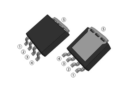
| Package (House Name) | LF |
| Package (JEDEC Code) | MO-235B similar |
| Storage temperature | -55 to 175 |
| Temperature1 | Tc |
| Temperrature2 | Tc |
| Thermal resistance | 0.89 |
| Other | |
| As | Non-USE |
| Automotive | YES |
| Based on AEC-Q101 | YES |
| Br | Non-USE |
| Conditions | VDD=32V, VGS=10V, ID=105A |
| conditions | IF=105A, VGS=0V, di/dt=100A/μs |
| Ctrl Number | P105LF4QLK_Rev.04(2021.10) |
| Diag01 | P105LF4QLK_01_VDS.jpg |
| Diag02 | P105LF4QLK_02_VGS.jpg |
| Diag03 | P105LF4QLK_03_Ron-ID.jpg |
| Diag04 | P105LF4QLK_04_Ron-Tc.jpg |
| Diag05 | P105LF4QLK_05_Vth.jpg |
| Diag06 | P105LF4QLK_06_SOA.jpg |
| Diag07 | P105LF4QLK_07_TTI.jpg |
| Diag08 | P105LF4QLK_08_C.jpg |
| Diag09 | P105LF4QLK_09_PD.jpg |
| Diag10 | P105LF4QLK_10_Qg.jpg |
| Diag11 | P105LF4QLK_11_DC.jpg |
| Diode reverse recovery charge | 45 |
| Diode reverse recovery time | 41 |
| Evidence | 5QE-188230-1.pdf |
| Forward transconductance | 20 |
| Gate to drain charge | 23 |
| Gate to source charge | 15.5 |
| I D | 105A |
| Input capacitance | 4090 |
| Ni | USE |
| Order Quantity | FAQをご確認ください。 |
| Output capacitance | 492 |
| Pb | USE |
| Polarity | N-channel |
| R DS(ON) (typ.) | 2.1mΩ |
| Reverce transfer capacitnce | 246 |
| Rp | Non-USE |
| Sb | Non-USE |
| Series | EETMOS4 |
| Single avalanche energy | 183 |
| Spec Code | 5071 |
| Static drain-source on-state resistance | 0.0043 |
| Total gate charge | 76 |
| V DSS | 40V |
| Vth(typ.) | 2.0V |