Analog Devices Inc./Maxim IntegratedUnited States
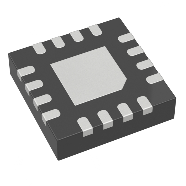
IC ADJ OV/OC PROTECTOR 16TQFN
MAX14588 is a 1A adjustable overcurrent and overvoltage protection IC with an input voltage range of 4.5V to 36V, featuring low 190mΩ(on) resistance, available in a 16-pin TQFN package, operating from -40°C to +125°C, with programmable current limiting and multiple fault response modes.Checked against the datasheet
All alternatives
View full reportTechnical parameters
Datasheet-verified parameters
25 items| Parameter | Value and test conditions | Source |
|---|---|---|
| Package | 16 TQFN-EP (3mm x 3mm) | |
| Operating Temperature Range | -40°C to +125°C | |
| RoHS | Compliant (+ denotes lead(Pb)-free package/RoHS-compliant package) | |
| IN Voltage | Min: 4.5V, Max: 36V | |
| Internal FETs On-Resistance | Typ: 190mΩ, Max: 370mΩ (I_LOAD=100mA, V_IN≥8V) | |
| Current-Limit Adjustment Range | Min: 0.15A, Max: 1.0A |
All parameters (13)
| Power | |
|---|---|
| Voltage - Clamping | - |
| Voltage - Working | 36V |
| Environment and package | |
| Mounting Type | Surface Mount |
| Package | Tape & Reel (TR) Cut Tape (CT) Digi-Reel® |
| Package / Case | 16-WFQFN Exposed Pad |
| Supplier Device Package | 16-TQFN (3x3) |
| Other | |
| Applications | General Purpose |
| Base Product Number | MAX14588 |
| Mfr | Analog Devices Inc./Maxim Integrated |
| Number of Circuits | 1 |
| Product Status | Active |
| Series | - |
| Technology | Internal Switch |
Pinout and package
\*CONNECT EP TO GND
| Pin | Name | Function | Source |
|---|---|---|---|
| 1 | CLTS_MODE: Current-Limit-Type Select Mode. 0: CLTS1 and CLTS2 sampled only when (V_IN - V_OUT) < 0.6V; 1: Continuously sampled. | ||
| 2 | CLHS: Current-Limit-Type-Select Logic-High Voltage. Connect CLTS_MODE/CLTS1/CLTS2 to CLHS for logic-high. | ||
| 3 | CLTS1: Current-Limit-Type Select 1. | ||
| 4 | CLTS2: Current-Limit-Type Select 2. | ||
| 5 | HVEN: 36V Capable Active-Low Enable Input. | ||
| 8 | OVLO: Externally Programmable Overvoltage Lockout Threshold. Connect OVLO to GND to use the default internal OVLO threshold. Connect OVLO to an external resistor-divider to define a threshold externally. | ||
| 9 | UVLO: Externally Programmable Undervoltage Lockout Threshold. Connect UVLO to GND to use the default internal UVLO threshold. Connect UVLO to an external resistor-divider to define a threshold externally. | ||
| 10 | SETI: Overload-Current-Limit Adjust. Connect a resistor from SETI to GND to program the overcurrent limit. SETI must be connected to a resistor. | ||
| 11 | GND: Ground. | ||
| 12 | FLAG: Open-Drain Fault Indicator Output. FLAG goes low when the fault duration exceeds the blanking time, reverse current is detected, thermal shutdown mode is active, OVLO threshold is reached, or SETI is connected to GND. | ||
| 13 | EN: Active-High Enable Input. | ||
| 16 | RIEN: Reverse-Current Enable Input. Connect RIEN to GND to disable the reverse-current flow protection. Connect RIEN to logic-high to activate the reverse-current flow protection. | ||
| 14, 15 | OUT: Output Voltage. Output of internal FETs. Bypass OUT to GND with a 1μF ceramic capacitor placed as close to the device as possible. | ||
| 6, 7 | IN: Overvoltage Protection Input. Bypass IN to ground with a 0.47μF ceramic capacitor. | ||
| EP | EP: Exposed Pad. Connect EP to ground. Do not use EP as the only ground connection. |
Documents
Datasheet-verified content is extracted by AI from the manufacturer datasheet. Click a page number to view the original.