Analog Devices Inc./Maxim IntegratedUnited States
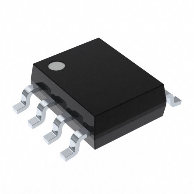
IC TRANSCEIVER HALF 1/1 8SOIC
MAX13488EESA+ is a +5V half-duplex RS-485 compatible transceiver with one driver and one receiver, supporting 16Mbps data rate, featuring AutoDirection control and hot-swap capability, in an 8-pin SO package, operating from -40°C to +85°C.Checked against the datasheet
All alternatives
View full reportTechnical parameters
Key specs
ProtocolRS-485
Drivers/Receivers1
Data rate16 MbpsMax
Supply voltage4.75 ~ 5.25 V
Datasheet-verified parameters
19 items| Parameter | Value and test conditions | Source |
|---|---|---|
| Protocol | RS-485 | |
| Drivers / Receivers | 1 Driver, 1 Receiver | |
| Data Rate | 16Mbps | |
| Supply Voltage | 4.75V to 5.25V (Typ 5V) | |
| Package | 8 SO | |
| Operating Temperature | -40°C to +85°C |
All parameters (16)
| Power | |
|---|---|
| Voltage - Supply | 4.75V ~ 5.25V |
| Environment and package | |
| Mounting Type | Surface Mount |
| Operating Temperature | -40°C ~ 85°C |
| Package | Tube |
| Package / Case | 8-SOIC (0.154", 3.90mm Width) |
| Supplier Device Package | 8-SOIC |
| Other | |
| Base Product Number | MAX13488 |
| Data Rate | 16Mbps |
| Duplex | Half |
| Mfr | Analog Devices Inc./Maxim Integrated |
| Number of Drivers/Receivers | 1/1 |
| Product Status | Active |
| Protocol | RS422, RS485 |
| Receiver Hysteresis | 25 mV |
| Series | - |
| Type | Transceiver |
Pinout and package
Package8 SO
| Pin | Name | Function | Source |
|---|---|---|---|
| 1 | RO: Receiver Output. When receiver is enabled and V(A) - V(B) > +200mV, RO is high. If V(A) - V(B) < -200mV, RO is low. | ||
| 2 | RE: Receiver Output Enable. Drive RE low to enable the RO. Drive RE high to let the AutoDirection circuit control the receiver. RE is a hot-swap input. | ||
| 3 | SHDN: Shutdown. Drive SHDN high to let the device operate in normal operation. Drive SHDN low to put the part in shutdown. | ||
| 4 | DI: Driver Input. Drive DI low to force noninverting output low and inverting output high. Drive DI high to force noninverting output high and inverting output low. DI is an input to the internal state machine that automatically enables and disables the driver. DI is a hot-swap input. | ||
| 5 | GND: Ground | ||
| 6 | A: Noninverting Receiver Input and Noninverting Driver Output | ||
| 7 | B: Inverting Receiver Input and Inverting Driver Output | ||
| 8 | VCC: Positive Supply, VCC = +5V ±5%. Bypass VCC to GND with a 0.1μF capacitor. |
Documents
Datasheet-verified content is extracted by AI from the manufacturer datasheet. Click a page number to view the original.