Texas InstrumentsUnited States

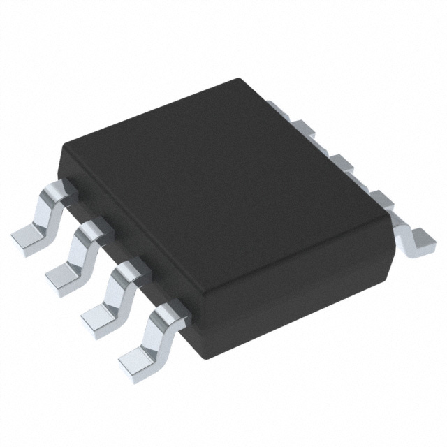
IC DDR-II TERM REG 8SOPWRPAD
LP2997MR/NOPB is a linear regulator for DDR-II SSTL-18 termination, outputting VTT = VDDQ/2 with 500mA continuous current, featuring thermal shutdown and Suspend To RAM, in SO PowerPAD-8 package.Checked against the datasheet
All alternatives
View full reportTechnical parameters
Datasheet-verified parameters
23 items| Parameter | Value and test conditions | Source |
|---|---|---|
| Package | SO PowerPAD (DDA), 8 Pins | |
| Operating Temperature | 0°C to +125°C | |
| RoHS | Yes | |
| VTT Output Voltage | PVIN = VDDQ = 1.8V, IOUT = 0A: Min 0.874V, Typ 0.908V, Max 0.939V | |
| VREF Voltage | PVIN = VDDQ = 1.8V: Min 0.887V, Typ 0.910V, Max 0.937V | |
| Quiescent Current | IOUT = 0A: Typ 320μA, Max 500μA |
All parameters (12)
| Power | |
|---|---|
| Current - Supply | 320µA |
| Voltage - Supply | 2.2V ~ 5.5V |
| Environment and package | |
| Mounting Type | Surface Mount |
| Operating Temperature | 0°C~125°C |
| Package | Tube |
| Package / Case | 8-PowerSOIC (0.154", 3.90mm Width) |
| Supplier Device Package | 8-SO PowerPad |
| Other | |
| Applications | DDR-II Terminator |
| Base Product Number | LP2997 |
| Mfr | Texas Instruments |
| Product Status | Active |
| Series | - |
Pinout and package
Figure 2. SO PowerPAD-8 Layout…
| Pin | Name | Function | Source |
|---|---|---|---|
| 1 | GND, Ground | ||
| 2 | SD, Shutdown (Active Low) | ||
| 3 | VSENSE, Feedback pin for regulating VTT | ||
| 4 | VREF, Buffered internal reference voltage of VDDQ/2 | ||
| 5 | VDDQ, Input for internal reference equal to VDDQ/2 | ||
| 6 | AVIN, Analog input pin | ||
| 7 | PVIN, Power input pin | ||
| 8 | VTT, Output voltage for connection to termination resistors | ||
| EP | EP, Exposed pad thermal connection, Connect to Ground |
Documents
Datasheet-verified content is extracted by AI from the manufacturer datasheet. Click a page number to view the original.