Texas InstrumentsUnited States

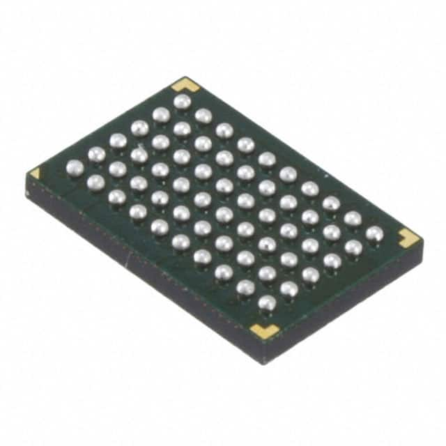
IC RF TXRX+MCU BLUETOOTH 60LFBGA
The LMX9830SMX/NOPB is a highly integrated Bluetooth 2.0 baseband controller and 2.4-GHz radio transceiver module in a 60-pin NFBGA package, supporting Class 2 operation with input sensitivity better than -80 dBm, and is RoHS compliantChecked against the datasheet
All alternatives
View full reportTechnical parameters
Datasheet-verified parameters
22 items| Parameter | Value and test conditions | Source |
|---|---|---|
| Package | NFBGA (60), 9.00 mm × 6.00 mm | |
| Ambient Operating Temperature Range | Min: -40 °C, Typ: 25 °C, Max: 125 °C | |
| RoHS | Green (RoHS & no Sb/Br) | |
| Halogen Free | Green (RoHS & no Sb/Br) | |
| Digital Voltage Regulator input | Min: 2.5 V, Typ: 2.75 V, Max: 3.6 V | |
| Supply Voltage Radio | Min: 2.5 V, Typ: 2.75 V, Max: 3 V |
All parameters (23)
| Power | |
|---|---|
| Current - Receiving | 65mA |
| Current - Transmitting | 65mA |
| Power - Output | 0dBm |
| Voltage - Supply | 2.5V ~ 3.6V |
| AC and DC characteristics | |
| Frequency | 2.4GHz |
| Environment and package | |
| Memory Size | 16kB RAM |
| Mounting Type | Surface Mount |
| Operating Temperature | -40°C~125°C |
| Package | Tape & Reel (TR); Cut Tape (CT); Digi-Reel® |
| Package / Case | 60-LFBGA |
| Supplier Device Package | 60-NFBGA (6x9) |
| Other | |
| Base Product Number | LMX9830 |
| Data Rate (Max) | 704kbps |
| GPIO | 3 |
| Mfr | Texas Instruments |
| Modulation | MSK |
| Product Status | Not For New Designs |
| Protocol | Bluetooth v2.0 |
| RF Family/Standard | Bluetooth |
| Sensitivity | -80dBm |
| Serial Interfaces | JTAG, SPI, UART |
| Series | - |
| Type | TxRx + MCU |
Pinout and package
NZB Package 60-Pin NFBGA Top V…
| Pin | Name | Function | Source |
|---|---|---|---|
| A1, A2, A3 | NC: No connect, for mechanical stability | ||
| A7 | PG6: GPIO | ||
| B2, E2 | GND: Ground | ||
| B6 | B_RESET_RA#: Buffered Reset Radio Output (active low) | ||
| C1 | OP6/SCL/MSK: ACCESS.Bus Clock / SPI Shift | ||
| C2 | CTS#: Host Serial Port Clear To Send (active low) | ||
| D1 | MDODI: SPI Master Out Slave In | ||
| D10 | ANT: RF Antenna, 50 Ω Nominal Impedance | ||
| D2 | PG7: GPIO - Default setup RF traffic LED indication | ||
| D3 | OP3/MWCS#: SPI Slave Select Input (active low) | ||
| D4 | OP7/SDA/MDIDO: ACCESS.Bus Serial Data / SPI Master In Slave Out |
Documents
Datasheet-verified content is extracted by AI from the manufacturer datasheet. Click a page number to view the original.