Texas InstrumentsUnited States

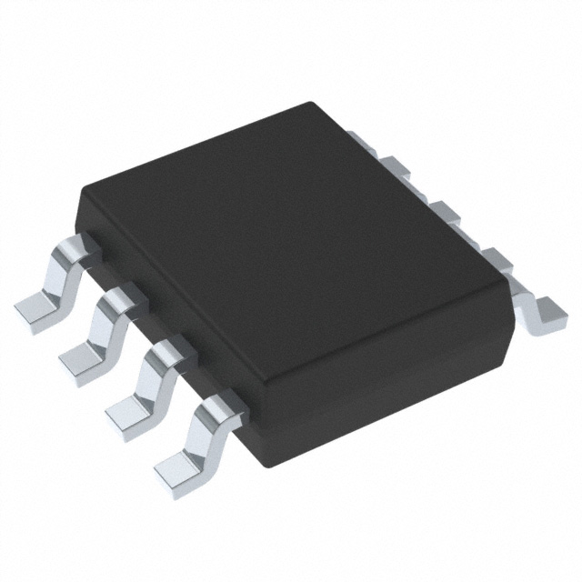
IC REG BUCK ADJ 600MA 8SOPWR
LM5017MRX/NOPB is a 100-V, 600-mA synchronous buck regulator in SO PowerPAD-8 package, with 7.5 V to 100 V input range, constant on-time control, and thermal shutdown protection.Checked against the datasheet
All alternatives
View full reportTechnical parameters
Key specs
Input voltage7.5 ~ 100 V
Output voltage1.225 ~ 90 V
Output current600 mAMax
Switching frequency1 MHz
Datasheet-verified parameters
23 items| Parameter | Value and test conditions | Source |
|---|---|---|
| Input voltage range | 7.5 V to 100 V | |
| Output current | 600 mA | |
| Package | SO PowerPAD (DDA) 8-Pin | |
| Operating temperature | -40°C to 125°C | |
| RoHS | Yes | |
| Recommended operating input voltage | Min: 7.5 V, Max: 100 V |
All parameters (21)
| Power | |
|---|---|
| Current - Output | 600mA |
| Voltage - Input (Max) | 100V |
| Voltage - Input (Min) | 7.5V |
| Voltage - Output (Max) | 90V |
| Voltage - Output (Min/Fixed) | 1.225V |
| AC and DC characteristics | |
| Frequency - Switching | Adj to 1MHz |
| Environment and package | |
| Mounting Type | Surface Mount |
| Operating Temperature | -40°C~125°C(TJ) |
| Package | Tape & Reel (TR); Cut Tape (CT); Digi-Reel® |
| Package / Case | 8-PowerSOIC (0.154", 3.90mm Width) |
| Supplier Device Package | 8-SO PowerPad |
| Other | |
| Base Product Number | LM5017 |
| Function | Step-Down |
| Mfr | Texas Instruments |
| Number of Outputs | 1 |
| Output Configuration | Positive |
| Output Type | Adjustable |
| Product Status | Active |
| Series | - |
| Synchronous Rectifier | Yes |
| Topology | Buck |
Pinout and package
Figure 5-1. DDA Package 8-Pin …
| Pin | Name | Function | Source |
|---|---|---|---|
| 1 | RTN, Ground connection | ||
| 2 | VIN, Input voltage | ||
| 3 | UVLO, Undervoltage comparator input | ||
| 4 | RON, On-time control | ||
| 5 | FB, Feedback | ||
| 6 | VCC, Output from the internal high-voltage series pass regulator | ||
| 7 | BST, Bootstrap capacitor | ||
| 8 | SW, Switching node | ||
| EP | EP, Exposed Pad, must be connected to the RTN pin |
Documents
Datasheet-verified content is extracted by AI from the manufacturer datasheet. Click a page number to view the original.