Texas InstrumentsUnited States

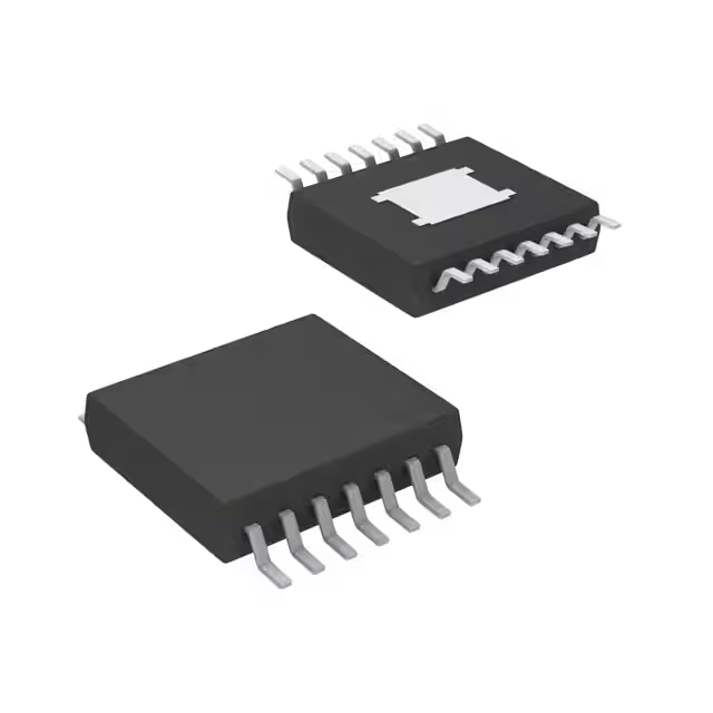
IC REG CTRLR BUCK 14TSSOP
LM3150MH/NOPB is a wide-VIN synchronous buck controller with 6V to 42V input range, up to 1MHz switching frequency, in HTSSOP-14 package, featuring COT control and multiple protection functions.Checked against the datasheet
All alternatives
View full report1 alternatives on file. Sign in to view them.
Technical parameters
Key specs
TopologyBuck
Outputs1
Input voltage6 ~ 42 V
Switching frequency1 MHz
Datasheet-verified parameters
20 items| Parameter | Value and test conditions | Source |
|---|---|---|
| Topology | Synchronous Buck | |
| Outputs | 1 | |
| Input Voltage Range | 6 V to 42 V | |
| Switching Frequency | up to 1 MHz | |
| Package | HTSSOP (14) | |
| Operating Temperature | -40 °C to 125 °C |
All parameters (22)
| Power | |
|---|---|
| Voltage - Supply (Vcc/Vdd) | 6V ~ 42V |
| AC and DC characteristics | |
| Frequency - Switching | Up to 1MHz |
| Environment and package | |
| Mounting Type | Surface Mount |
| Operating Temperature | -40°C~125°C(TJ) |
| Package | Tube |
| Package / Case | 14-TSSOP (0.173", 4.40mm Width) Exposed Pad |
| Supplier Device Package | 14-HTSSOP |
| Other | |
| Base Product Number | LM3150 |
| Clock Sync | No |
| Control Features | Current Limit, Enable, On Time Control, Soft Start |
| Duty Cycle (Max) | - |
| Function | Step-Down |
| Mfr | Texas Instruments |
| Number of Outputs | 1 |
| Output Configuration | Positive |
| Output Phases | 1 |
| Output Type | Transistor Driver |
| Product Status | Active |
| Serial Interfaces | - |
| Series | SIMPLE SWITCHER® |
| Synchronous Rectifier | Yes |
| Topology | Buck |
Pinout and package
HTSSOP PWP 14 PINS Top View
| Pin | Name | Function | Source |
|---|---|---|---|
| 1 | VCC: Supply Voltage for FET Drivers, nominally regulated to 5.95 V | ||
| 2 | VIN: Input Supply Voltage, nominal input range is 6 V to 42 V | ||
| 3 | EN: Enable, apply logic high > 1.26 V typ or leave floating to enable, ground to disable | ||
| 4 | FB: Feedback, internally connected to regulation, overvoltage, and short-circuit comparators, regulation setting is 0.6 V | ||
| 5 | SGND: Signal Ground, ground for all internal bias and reference circuitry, should be connected to PGND at a single point | ||
| 6 | SS: Soft-Start, an internal 7.7-μA current source charges an external capacitor to provide the soft-start function | ||
| 7 | RON: On-time Control, an external resistor from VIN to this pin sets the high-side switch on-time | ||
| 8 | ILIM: Current Limit, monitors current through the low-side switch and triggers current limit operation if the inductor valley current exceeds a user defined value | ||
| 9 | SGND: Signal Ground, ground for all internal bias and reference circuitry, should be connected to PGND at a single point | ||
| 10 | SW: Switch Node, switch pin of controller and high-gate driver lower supply rail, a boost capacitor is also connected between this pin and BST pin | ||
| 11 | HG: High-Side Gate Drive, gate drive signal to the high-side NMOS switch, voltage supplied by the differential voltage between the BST pin and SW pin | ||
| 12 | BST: Connection for Bootstrap Capacitor, high-gate driver upper supply rail, connect a 0.33 to 0.47-μF capacitor from SW pin to this pin | ||
| 13 | LG: Low-Side Gate Drive, gate drive signal to the low-side NMOS switch, voltage supplied by VCC | ||
| 14 | PGND: Power Ground, synchronous rectifier MOSFET source connection, tie to power ground plane, should be tied to SGND at a single point | ||
| EP | EP: Exposed Pad, exposed die attach pad should be connected directly to SGND, also used to help dissipate heat out of the IC |
Documents
Datasheet-verified content is extracted by AI from the manufacturer datasheet. Click a page number to view the original.