Microchip TechnologyUnited States
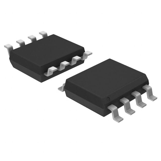
IC LED DRIVER CTRLR PWM 8SOIC
HV9910CLG-G is an open-loop current-mode LED driver IC with an internal 15-450V linear regulator, supporting PWM and linear dimming, featuring over-temperature protection in an 8-lead SOIC package.Checked against the datasheet
All alternatives
View full report5 alternatives on file, including 1 Chinese alternatives. Sign in to view them.
Technical parameters
Key specs
TopologyBuck
Outputs1
Input voltage15 ~ 450 V
Datasheet-verified parameters
14 items| Parameter | Value and test conditions | Source |
|---|---|---|
| Topology | Open loop peak current controller | |
| Input DC supply voltage range | Min: 15 V, Max: 450 V | |
| Package | 8-lead SOIC | |
| Operating Ambient Temperature | -40°C < TA < +125°C | |
| RoHS | Lead (Pb)-free/ROHS-compliant | |
| Internally regulated voltage | Min: 7.25 V, Typ: 7.50 V, Max: 7.75 V (VIN=15V, I_DD(ext)=0, PWMD=VDD, 500pF at GATE, ROSC=249kΩ) |
All parameters (20)
| Power | |
|---|---|
| Current - Output / Channel | - |
| Voltage - Output | - |
| Voltage - Supply (Max) | 450V |
| Voltage - Supply (Min) | 15V |
| AC and DC characteristics | |
| Frequency | 25kHz, 100kHz |
| Environment and package | |
| Mounting Type | Surface Mount |
| Operating Temperature | -40°C~125°C(TJ) |
| Package | Tape & Reel (TR); Cut Tape (CT); Digi-Reel® |
| Package / Case | 8-SOIC (0.154", 3.90mm Width) |
| Supplier Device Package | 8-SOIC |
| Other | |
| Applications | Backlight, Lighting, Signage |
| Base Product Number | HV9910 |
| Dimming | Analog, PWM |
| Internal Switch(s) | No |
| Mfr | Microchip Technology |
| Number of Outputs | 1 |
| Product Status | Active |
| Series | - |
| Topology | Step-Down (Buck) |
| Type | DC DC Controller |
Pinout and package
Pin Diagram 8-Lead SOIC
| Pin | Name | Function | Source |
|---|---|---|---|
| 1 | VIN: Input of an 15 - 450V linear regulator. | ||
| 2 | CS: Current sense pin used to sense the FET current by means of an external sense resistor. When this pin exceeds the lower of either the internal 250mV or the voltage at the LD pin, the GATE output goes low. | ||
| 3 | GND: Ground return for all internal circuitry. Must be electrically connected to the power ground. | ||
| 4 | GATE: Output GATE driver for an external N-channel power MOSFET. | ||
| 5 | PWMD: TTL-compatible, PWM-dimming input of the IC. When this pin is pulled to GND or left open, the GATE driver is turned off. When the pin is pulled high, the GATE driver operates normally. | ||
| 6 | VDD: Power supply pin for all internal circuits. It must be bypassed with a low ESR capacitor to GND (≥ 0.1μF). | ||
| 7 | LD: Linear-dimming input and sets the current sense threshold as long as the voltage at the pin is less than 250mV (typ). | ||
| 8 | RT: Sets the oscillator frequency. When a resistor is connected between RT and GND, the HV9910C operates in constant frequency mode. When the resistor is connected between RT and GATE, the IC operates in constant off-time mode. |
Documents
Datasheet-verified content is extracted by AI from the manufacturer datasheet. Click a page number to view the original.