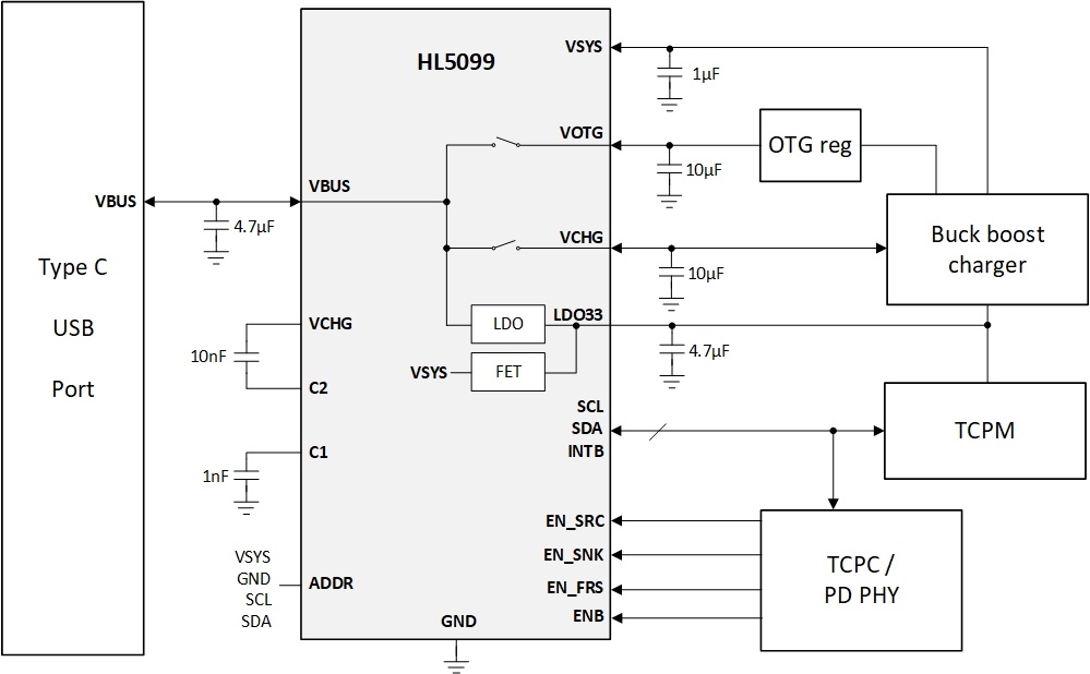
The HL5099 provides a dual channel VBUS power switches and 3.3V LDO for USB PD application. The device includes a bidirectional high voltage switch which supports up to 22V sink and 6V source voltage, VOTG switch supporting up to 13.2V source voltage and a 100mA 3.3V LDO providing power supply to PD controller in dead battery operation. Between VBUS and VCHG, back-to-back high voltage switches (HVSW) is implemented, and its AMR is 28V for both pins. The integrated power switch can be configured as a bi-directional switch with an appropriate I2C control or enable pins. In the SINK mode, allowable current is continuous 7A. In the source mode, switch current flows from VCHG to VBUS and maximum allowable current is 3A. From the VOTG to VBUS (VOTG mode), there is back-to-back power switch which AMR is 16V on VOTG. This switch is to source power from VOTG to VBUS up to 13.2V and 3A continuous current. This power switch has an ideal diode feature and supports fast role swap for USB PD3.0 application. HL5099 has built-in protections, programmable VBUS over voltage protection, reverse current protection, short current protection, programmable overcurrent protection in SOURCE / VOTG modes, Over temperature protection. VBUS discharge circuit is integrated to meet USB PD VBUS discharging requirement. To decrease inrush current during normal startup, turn on slew rate control has been built in for both power switches. It is also possible to set the various parameter and monitor the status of the HL5099 using I2C communication. Source switch selection, OVP threshold and Current Limit Protection level could be set through I2C communication. Various device status could be monitored using I2C including device modes (SINK/SRC/VOTG), protection flag.The HL5099 is available in a 42-pin WLCSP package.
All alternatives
View full reportTechnical parameters
No technical parameters are available for this part.