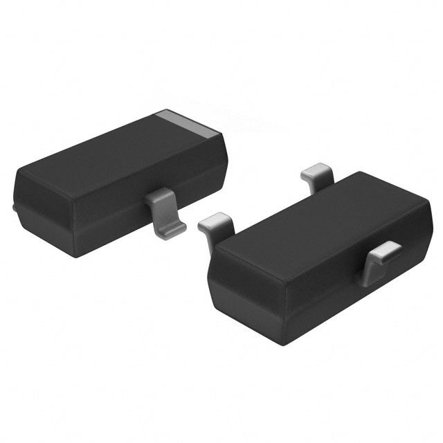
Alpha & Omega Semiconductor Inc.United States
MOSFET P-CH 30V 4A SOT23-3L
AO3401A is a 30V P-channel MOSFET in SOT23 package, featuring low on-resistance and low gate charge, suitable for load switches and general applications.Checked against the datasheet
All alternatives
View full report62 alternatives on file, including 16 Chinese alternatives. Sign in to view them.
Technical parameters
Key specs
ChannelP-channel
Drain-source voltage-30 V
Continuous drain current-4 AMax -4 A (TA=25°C),Max -3.2 A (TA=70°C)
On-resistance50 mΩMax · Max 50 mΩ (VGS=-10V,ID=-4.0A)
Gate threshold voltage-1.3 VMax · Max -1.3 V (VDS=VGS,ID=-250μA)
Datasheet-verified parameters
28 items| Parameter | Value and test conditions | Source |
|---|---|---|
| Channel | P-Channel | |
| Drain-Source Voltage | Max -30 V | |
| Continuous Drain Current | Max -4 A (TA=25°C), Max -3.2 A (TA=70°C) | |
| Static Drain-Source On-Resistance | Typ 41 mΩ, Max 50 mΩ (VGS=-10V, ID=-4.0A) | |
| Gate Threshold Voltage | Min -0.5 V, Typ -0.9 V, Max -1.3 V (VDS=VGS, ID=-250μA) | |
| Package | SOT23 |
All parameters (21)
| Power | |
|---|---|
| Current - Continuous Drain (Id) @ 25°C | 4A (Ta) |
| Drain to Source Voltage (Vdss) | 30 V |
| Drive Voltage (Max Rds On, Min Rds On) | 2.5V, 10V |
| Power Dissipation (Max) | 1.4W (Ta) |
| Environment and package | |
| Mounting Type | Surface Mount |
| Operating Temperature | -55°C~150°C(TJ) |
| Package | Tape & Reel (TR); Cut Tape (CT); Digi-Reel® |
| Package / Case | 3-SMD, SOT-23-3 Variant |
| Supplier Device Package | SOT-23-3 |
| Other | |
| Base Product Number | AO3401 |
| FET Feature | - |
| FET Type | P-Channel |
| Gate Charge (Qg) (Max) @ Vgs | 12.2 nC @ 4.5 V |
| Input Capacitance (Ciss) (Max) @ Vds | 1200 pF @ 15 V |
| Mfr | Alpha & Omega Semiconductor Inc. |
| Product Status | Not For New Designs |
| Rds On (Max) @ Id, Vgs | 44mOhm @ 4.3A, 10V |
| Series | - |
| Technology | MOSFET (Metal Oxide) |
| Vgs (Max) | ±12V |
| Vgs(th) (Max) @ Id | 1.3V @ 250µA |
Documents
DatasheetDatasheet · 318.9 KB · 2026-11-09DatasheetDatasheet · 316.8 KB · 2026-11-09DatasheetDatasheet · 534.9 KB · 2026-09-21DatasheetDatasheet · 231.1 KB · 2026-09-21Package DrawingPackage Drawing · 399.2 KB · 2026-09-22Package DrawingPackage Drawing · 269.9 KB · 2026-09-22Package DrawingPackage Drawing · 138.4 KB · 2026-09-22Quality & ReliabilityQuality & Reliability · 115.8 KB · 2026-09-22
Open document centerDatasheet-verified content is extracted by AI from the manufacturer datasheet. Click a page number to view the original.