Analog Devices Inc.United States
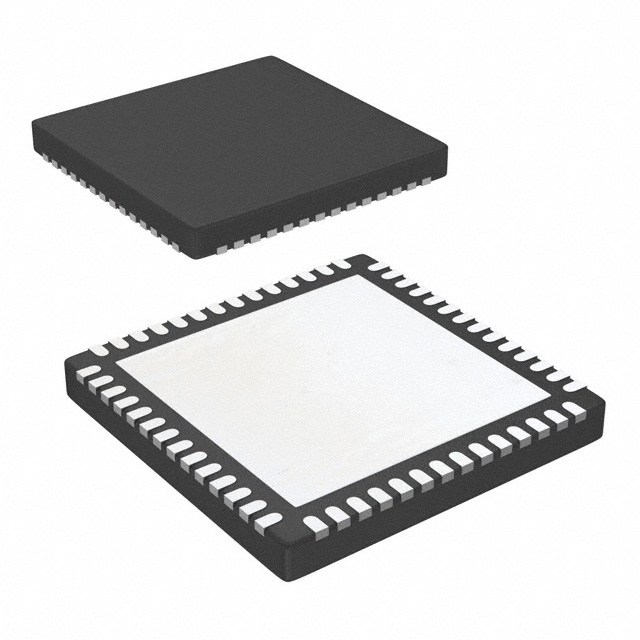
RF MODULATOR 100MHZ-2.4GHZ 56QFN
ADRF6755ACPZ is a 100 MHz to 2400 MHz I/Q modulator with integrated fractional-N PLL and VCO, 47 dB gain control span, in a 56-lead LFCSP package, operating from -40°C to +85°C.Checked against the datasheet
All alternatives
View full reportTechnical parameters
Datasheet-verified parameters
20 items| Parameter | Value and test conditions | Source |
|---|---|---|
| Package | 56-Lead Lead Frame Chip Scale Package [LFCSP_VQ], Tray, CP-56-4 | |
| Operating Temperature Range | -40°C to +85°C | |
| RoHS Compliance | RoHS Compliant Part (Z) | |
| Output Frequency Range | 100 MHz to 2400 MHz | |
| Gain Control Span | 47 dB in 1 dB steps | |
| Output 1 dB Compression | 8 dBm at LO = 1800 MHz |
All parameters (17)
| Power | |
|---|---|
| Current - Supply | 380 mA |
| Output Power | -1.7dBm |
| Voltage - Supply | 4.75V ~ 5.25V |
| AC and DC characteristics | |
| LO Frequency | - |
| Noise Floor | -160.5dBm/Hz |
| RF Frequency | 100MHz ~ 2.4GHz |
| Test Frequency | 100MHz |
| Environment and package | |
| Mounting Type | Surface Mount |
| Package | Tray |
| Package / Case | 56-VFQFN Exposed Pad, CSP |
| Supplier Device Package | 56-LFCSP-VQ (8x7.75) |
| Other | |
| Base Product Number | ADRF6755 |
| Function | Modulator |
| Mfr | Analog Devices Inc. |
| P1dB | 9dBm |
| Product Status | Active |
| Series | - |
Pinout and package
Package56-Lead Lead Frame Chip Scale Package [LFCSP_VQ], Tray, CP-56-4
| Pin | Name | Function | Source |
|---|---|---|---|
| 1 | VCC1: Positive Power Supply for I/Q Modulator | ||
| 2 | IBB: Differential In-Phase Baseband Input | ||
| 3 | IBB: Differential In-Phase Baseband Input (Inverted) | ||
| 4 | QBB: Differential Quadrature Baseband Input (Inverted) | ||
| 5 | QBB: Differential Quadrature Baseband Input | ||
| 6 | AGND: Analog Ground | ||
| 7 | RSET: Charge Pump Current Set | ||
| 8 | NC: No Connect | ||
| 9 | CP: Charge Pump Output | ||
| 10 | NC: No Connect | ||
| 11 | VCC1: Positive Power Supply for I/Q Modulator | ||
| 12 | REGOUT: 3.3 V Output Supply | ||
| 13 | VREG1: Positive Power Supply for PLL Synthesizer, VCO, and Serial Port | ||
| 14 | VREG2: Positive Power Supply for PLL Synthesizer, VCO, and Serial Port | ||
| 15 | VREG3: Positive Power Supply for PLL Synthesizer, VCO, and Serial Port | ||
| 16 | VREG4: Positive Power Supply for PLL Synthesizer, VCO, and Serial Port | ||
| 17 | REFIN: Reference Input | ||
| 18 | REFIN: Reference Input Bar | ||
| 19 | AGND: Analog Ground | ||
| 20 | AGND: Analog Ground | ||
| 21 | AGND: Analog Ground | ||
| 22 | AGND: Analog Ground | ||
| 23 | AGND: Analog Ground | ||
| 24 | AGND: Analog Ground | ||
| 25 | LOMON: Differential Monitor Output | ||
| 26 | LOMON: Differential Monitor Output (Inverted) | ||
| 27 | CS: Chip Select, CMOS Input | ||
| 28 | SDO: Serial Data Output for SPI Port | ||
| 29 | SDI/SDA: Serial Data Input for SPI Port/Serial Data Input/Output for I2C Port | ||
| 30 | CLK/SCL: Serial Clock Input for SPI/I2C Port | ||
| 31 | VREG5: Positive Power Supply for PLL Synthesizer, VCO, and Serial Port | ||
| 32 | DGND: Digital Ground | ||
| 33 | CCOMP1: Internal Compensation Node | ||
| 34 | CCOMP2: Internal Compensation Node | ||
| 35 | CCOMP3: Internal Compensation Node | ||
| 36 | VREG6: Positive Power Supply for PLL Synthesizer, VCO, and Serial Port | ||
| 37 | AGND: Analog Ground | ||
| 38 | VTUNE: Control Input to the VCO | ||
| 39 | AGND: Analog Ground | ||
| 40 | AGND: Analog Ground | ||
| 41 | VCC3: Positive Power Supply for I/Q Modulator | ||
| 42 | VCC3: Positive Power Supply for I/Q Modulator | ||
| 43 | MUXOUT: Mux Output, for diagnostic use only | ||
| 44 | LDET: Lock Detect | ||
| 45 | TXDIS: Output Disable | ||
| 46 | AGND: Analog Ground | ||
| 47 | AGND: Analog Ground | ||
| 48 | RFOUT: RF Output, Single-ended, 50 Ω, internally biased | ||
| 49 | AGND: Analog Ground | ||
| 50 | AGND: Analog Ground | ||
| 51 | AGND: Analog Ground | ||
| 52 | AGND: Analog Ground | ||
| 53 | AGND: Analog Ground | ||
| 54 | AGND: Analog Ground | ||
| 55 | VCC2: Positive Power Supply for I/Q Modulator | ||
| 56 | VCC2: Positive Power Supply for I/Q Modulator | ||
| EP | EP: Exposed Paddle, Connect to ground plane via a low impedance path |
Documents
Datasheet-verified content is extracted by AI from the manufacturer datasheet. Click a page number to view the original.