时钟数据恢复(CDR)
共 50+ 条- 匹配型号50+
- 有数据手册(前 50 条中)17
- 涉及品牌(前 50 条中)2
产品搜索结果共 50+ 条
| 对比 | 产品型号 | 品牌 | 分类 | 产品描述 | 技术资料 | 替代 | 操作 |
|---|---|---|---|---|---|---|---|
| 时钟数据恢复(CDR) | 数据手册2 | 查看详情 | |||||
| 时钟数据恢复(CDR) | The MAX3876 is a compact, low-power clock recovery and data retiming IC for 2.488Gbps SDH/SONET applications. The fully integrated phase-locked loop (PLL) recovers a synchronous clock signal from the serial NRZ data input. The data is retimed by the recovered clock. Differential CML outputs are provided for both clock and data signals, and an additional 2.488Gbps serial input is available for system loopback diagnostic testing. The device also includes a TTL-compatible loss-of-lock (active-low LOL) monitor. The MAX3876 is designed for both section-regenerator and terminal-receiver applications in OC-48/STM-16 transmission systems. Its jitter performance exceeds all of the SONET/SDH specifications. This device operates from a +3.3V or +5.0V single supply over a -40°C to +85°C temperature range. Power consumption is typically only 445mW with a +3.3V supply. The MAX3876 is available in a 32-pin TQFP package as well as in die form. Applications 2.488Gbps ATM Receivers Add/Drop Multiplexers Digital Cross-Connects Digital Video Transmission Intrarack/Subrack Interconnects SDH/SONET Receivers and Regenerators SDH/SONET Test Equipment | 数据手册1 | 查看详情 | ||||
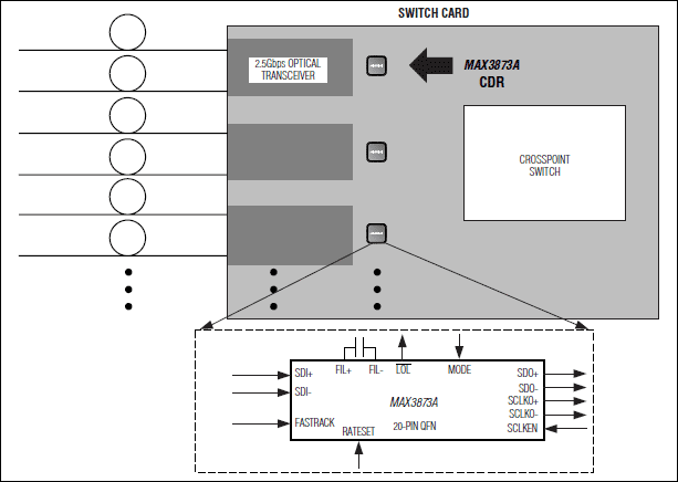
| 时钟数据恢复(CDR) | The MAX3873A is a compact, low-power 2.488Gbps/2.67Gbps clock-recovery and data-retiming IC for SDH/SONET applications. The phase-locked loop (PLL) recovers a synchronous clock signal from the serial NRZ data input. The input data is then retimed by this recovered clock, providing a clean data output. The MAX3873A meets all SDH/SONET jitter specifications, does not require an external reference clock to aid in frequency acquisition, and provides excellent tolerance to both deterministic and sinusoidal jitter. The MAX3873A provides a PLL loss-of-lock (active-low LOL) output to indicate whether the CDR is in lock. The recovered data and clock outputs are CML with on-chip 50Ω back terminations on each line. The clock output can be powered down if not used. The MAX3873A is implemented in Maxim's second-generation SiGe process and consumes only 260mW at 3.3V supply (output clock disabled, low output swing). The device is available in a 4mm x 4mm 20-pin QFN exposed-pad package and operates from -40°C to +85°C. Applications Add/Drop Multiplexers Digital Cross-Connects DWDM Transmission Systems SDH/SONET Receivers and Regenerators SDH/SONET Test Equipment Switch Matrix Backplanes | 数据手册1 | 查看详情 | ||||
| 时钟数据恢复(CDR) | The MAX3877/MAX3878 are compact, low-power clock recovery and data retiming ICs for 2.488Gbps SONET/ SDH applications. The fully integrated phase-locked loop (PLL) recovers a synchronous clock signal from the serial NRZ data input, which is retimed by the recovered clock. An additional 2.488Gbps serial input is available for system loopback diagnostic testing, or this input can be connected to a 155MHz reference clock to maintain a valid clock output in the absence of data transitions. The MAX3877/MAX3878 provide vertical threshold and phase-adjust control to optimize system BER in DWDM applications. These devices provide both loss-of-lock (active-low LOL) and loss-of-signal (LOS) monitors. Differential CML outputs are provided for both clock and data signals on the MAX3877, and differential PECL outputs are provided for clock and data signals on the MAX3878. The MAX3877/MAX3878 are designed for both section-regenerator and terminal-receiver applications in OC-48/STM-16 transmission systems. Their jitter performance exceeds all of the SONET/SDH specifications. These devices operate from a single +3.0V to +3.6V supply over a -40°C to +85°C temperature range. Typical power consumption is only 540mW with a +3.3V supply (MAX3878). They are available in a 32-pin TQFP-EP package with an exposed pad, as well as in die form. Applications Controllers | 数据手册1 | 查看详情 | ||||
| 时钟数据恢复(CDR) | The MAX3886 2.488Gbps/1.244Gbps/622Mbps CDR with SerDes (serializer/deserializer) is designed specifically for low-cost optical network terminal (ONT) applications in Gigabit passive optical network (GPON) and broadband passive optical network (BPON) fiber-to-the-home (FTTH) systems. It provides G.984- and G.983-compliant clock and data recovery (CDR) for the continuous downstream data signal, with an integrated 4-bit SerDes that has LVDS parallel interfaces and CML serial interfaces. The SerDes uses the recovered downstream clock for upstream serialization (loopback clock), providing optimum PON operation. The CDR frequency reference can be provided by a low-cost 19.44MHz SMD-type crystal or external LVCMOS source, and excellent jitter tolerance supports applications requiring FEC. An integrated burst-enable signal path also simplifies high-performance upstream burst timing. This 3.3V IC is housed in a 8mm x 8mm, 56-lead thin QFN package and operates from -40°C to +85°C. Applications BPON/GPON Optical Network Terminal (ONT) | 数据手册1 | 查看详情 | ||||
| 时钟数据恢复(CDR) | The MAX3875 is a compact, low-power clock recovery and data retiming IC for 2.488Gbps SDH/SONET applications. The fully integrated phase-locked loop recovers a synchronous clock signal from the serial NRZ data input, which is retimed by the recovered clock. Differential PECL-compatible outputs are provided for both clock and data signals, and an additional 2.488Gbps serial input is available for system loopback diagnostic testing. The device also includes a TTL-compatible loss-of-lock (LOL-bar) monitor. The MAX3875 is designed for both section-regenerator and terminal-receiver applications in OC-48/STM-16 transmission systems. Its jitter performance exceeds all of the SONET/SDH specifications. This device operates from a single +3.3V to +5.0V supply over a -40°C to +85°C temperature range. The typical power consumption is only 400mW with a +3.3V supply. It is available in a 32-pin TQFP package, as well as in die form. Applications 2.488Gbps ATM Receivers Add/Drop Multiplexers Digital Cross-Connects Digital Video Transmission SDH/SONET Receivers and Regenerators SDH/SONET Test Equipment | 数据手册1 | 查看详情 | ||||
| 时钟数据恢复(CDR) | The ADN2813 provides the receiver functions of quantization, signal level detect, and clock and data recovery for continuous data rates from 12.3 Mb/s to 1.25 Gb/s. The ADN2813 automatically locks to all data rates without the need for an external reference clock or programming. All SONET jitter requirements are met, including jitter transfer, jitter generation, and jitter tolerance. All specifications are quoted for −40°C to +85°C ambient temperature, unless otherwise noted. This device, together with a PIN diode and a TIA preamplifier, can implement a highly integrated, low cost, low power fiber optic receiver. The receiver front end loss of signal (LOS) detector circuit indicates when the input signal level has fallen below a useradjustable threshold. The LOS detect circuit has hysteresis to prevent chatter at the output. The ADN2813 is available in a compact 5 mm × 5 mm 32-lead chip scale package. Applications SONET OC-1/3/12 and all associated FEC rates Fibre Channel, GbE, HDTV, etc. WDM transponders Regenerators/repeaters Test equipment Broadband cross-connects and routers | 数据手册2 | 查看详情 | ||||
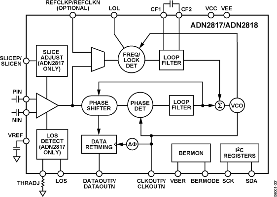
| 时钟数据恢复(CDR) | The ADN2817 /ADN2818 provide the receiver functions of quantization, signal level detect, and clock and data recovery for continuous data rates from 10 Mbps to 2.7 Gbps. The ADN2817/ ADN2818 automatically lock to all data rates without the need for an external reference clock or programming. All SONET jitter requirements are exceeded, including jitter transfer, jitter generation, and jitter tolerance. All specifications are quoted for −40°C to +85°C ambient temperature, unless otherwise noted. This device, together with a PIN diode and a TIA preamplifier, can implement a highly integrated, low cost, and low power fiber optic receiver. The ADN2817/ADN2818 have many optional features available through an I 2 C interface. For example, the user can read back the data rate onto which the ADN2817 or ADN2818 is locked, or the user can set the device to lock only to one particular data rate if provisioning of data rates is required. A BERMON circuit provides an estimate of the received bit error rate (BER) without interruption of the data. Alternatively, the user can adjust the data sampling phase to optimize the received BER. The ADN2817/ADN2818 are available in a compact 5 mm × 5 mm, 32-lead, lead frame chip scale package. Applications SONET OC-1, OC-3, OC-12, OC-48, and all associated FEC rates Fibre Channel, 2× Fibre Channel, GbE, HDTV, and others WDM transponders Regenerators/repeaters Test equipment | 数据手册2 | 查看详情 | ||||
| 时钟数据恢复(CDR) | The MAX3675 is a complete clock-recovery and data-retiming IC incorporating a limiting amplifier. It is intended for 622Mbps SDH/SONET applications and operates from a single +3.3V supply. The MAX3675 has two differential input amplifiers: one accepts PECL levels, while the other accepts small-signal analog levels. The analog inputs access the limiting amplifier stage, which provides both a received-signal-strength indicator (RSSI) and a programmable-threshold loss-of-power (LOP) monitor. Selecting the PECL amplifier disables the limiting amplifier, conserving power. A loss-of-lock (LOL) monitor is also incorporated as part of the fully integrated PLL. Applications Add/Drop Multiplexers ATM Switches Digital Cross-Connects SDH/SONET Access Nodes SDH/SONET Transmission Systems | 数据手册1 | 查看详情 | ||||
| 时钟数据恢复(CDR) | The MAX3270 is a complete Clock Recovery and Data Retiming IC for 155Mbps and 622Mbps SDH/SONET and ATM applications. The MAX3270 meets Bellcore and CCITT jitter tolerance specifications ensuring error-free data recovery. Recovered clock and data are phase aligned using a fully integrated phase-locked loop (PLL). An output frequency monitor (FM) is included to detect loss of PLL acquisition or a loss of input data. The MAX3270 has differential ECL input and output interfaces, so it is less susceptible to noise in a high-frequency environment. The fully integrated PLL includes an integrated phase-frequency detector that eliminates the need for external references. Applications 155Mbps (STM-1/OC-3) SDH/SONET Transmission Systems 155Mbps/622Mbps ATM/SONET Access Nodes 622Mbps (STM-4/OC-12) SDH/SONET Transmission Systems Add/Drop Multiplexers Cross-Connects | 数据手册1 | 查看详情 | ||||
| 时钟数据恢复(CDR) | Obsolete product page | 查看详情 | |||||
| 时钟数据恢复(CDR) | The ADN2806 provides the receiver functions for clock and data recovery, and data retiming for 622 Mbps NRZ data. The ADN2806 automatically locks to 622 Mbps data without the need for an external reference clock or programming. In the absence of input data, the output clock drifts no more than ±5%. All SONET jitter requirements are met, including jitter transfer, jitter generation, and jitter tolerance. All specifications are quoted for −40°C to +85°C ambient temperature, unless otherwise noted. This device, together with a PIN diode, TIA preamplifier, and a lim amp can implement a highly integrated, low cost, low power fiber optic receiver. The ADN2806 is available in a compact 5 mm × 5 mm, 32-lead LFCSP. Applications BPON ONT SONET OC-12 WDM transponders Regenerators/repeaters Test equipment Broadband cross-connects and routers | 数据手册2 | 查看详情 | ||||
| 时钟数据恢复(CDR) | The MAX3991 is a 10Gbps clock and data recovery (CDR) with limiting amplifier IC for XFP optical receivers. The MAX3991 and the MAX3992 (CDR with equalizer) form a signal conditioner chipset for use in XFP transceiver modules. The chipset is XFI compliant and offers multirate operation for data rates from 9.95Gbps to 11.1Gbps. The MAX3991 has 7mV P-P input sensitivity (BER < 10 -12 ), which allows direct connection to a transimpedance amplifier without the use of a stand-alone limiting amplifier. The phase-locked loop (PLL) is optimized for jitter tolerance and provides 0.6UI of high-frequency tolerance in SONET, Ethernet, and Fibre-Channel applications. The MAX3991 output provides 27% margin to the XFP eye mask specification. An AC-based power detector toggles the loss-of-signal (LOS) output when the input signal swing is below the user-programmed assert threshold. An external reference clock, with frequency equal to 1/64 or 1/16 of the serial data rate is used to aid in frequency acquisition. A loss-of-lock (LOL) indicator is provided to indicate the lock status of the receiver PLL. The MAX3991 is available in a 4mm x 4mm, 24-pin QFN package. It consumes 350mW from a single +3.3V supply and operates over the 0°C to +85°C temperature range. Applications 10.3Gbps/11.1Gbps Ethernet XFP Transceivers 10.5Gbps Fibre Channel XFP Transceivers 10Gbps DWDM Transceivers 9.95Gbps to 11.1Gbps Optical XFP Modules SONET OC-192/SDH STM-64 XFP Transceivers | 数据手册1 | 查看详情 | ||||
| 时钟数据恢复(CDR) | The MAX3873 is a compact, low-power 2.488Gbps/ 2.67Gbps clock-recovery and data-retiming IC for SDH/SONET applications. The phase-locked loop (PLL) recovers a synchronous clock signal from the serial NRZ data input. The input data is then retimed by this recovered clock, providing a clean data output. The MAX3873 meets all SDH/SONET jitter specifications, does not require an external reference clock to aid in frequency acquisition, and provides excellent tolerance to both deterministic and sinusoidal jitter. The MAX3873 provides a PLL loss-of-lock (LOL-bar) output to indicate whether the CDR is in lock. The recovered data and clock outputs are CML with on-chip 50Ω back terminations on each line. The clock output can be powered down if not used. The MAX3873 is implemented in Maxim's second-generation SiGe process and consumes only 260mW at 3.3V supply (output clock disabled, low output swing). The device is available in a 4mm x 4mm 20-pin QFN exposed-pad package and operates from -40¡ÆC to +85¡ÆC. Applications Add/Drop Multiplexers Digital Cross-Connects DWDM Transmission Systems SDH/SONET Receivers and Regenerators SDH/SONET Test Equipment Switch Matrix Backplanes | 数据手册1 | 查看详情 | ||||
| 时钟数据恢复(CDR) | The ADN2913 provides the receiver functions of quantization, signal level detection, and clock and data recovery for continuous data rates from 6.5 Mbps to 8.5 Gbps. The ADN2913 automatically locks to all data rates without the need for an external reference clock or programming. ADN2913 jitter performance exceeds all jitter specifications required by SONET/SDH, including jitter transfer, jitter generation, and jitter tolerance. The ADN2913 provides manual or automatic slice adjust and manual sample phase adjusts. Additionally, the user can select a limiting amplifier, equalizer, or 0 dB EQ at the input. The equalizer is adaptive or it can be manually set. The receiver front-end loss of signal (LOS) detector circuit indicates when the input signal level falls below a user-programmable threshold. The LOS detection circuit has hysteresis to prevent chatter at the LOS output. In addition, the input signal strength can be read through the I 2 C registers. The ADN2913 also supports pseudorandom binary sequence (PRBS) generation, bit error detection, and input data rate readback features. The ADN2913 is available in a compact 4 mm × 4 mm, 24-lead lead frame chip scale package (LFCSP). All ADN2913 specifications are defined over the ambient temperature range of −40°C to +85°C, unless otherwise noted. Applications SONET/SDH OC-1/OC-3/OC-12/OC-48 and all associated FEC rates 1GE, 1GFC, 2GFC, 4GFC, 8GFC, CPRI OS/L.6 up to OS/L.60 Any rate regenerators/repeaters | 数据手册2 | 查看详情 | ||||
| 时钟数据恢复(CDR) | The AD807 provides the receiver functions of data quantization, signal level detect, clock recovery and data retiming for 155 Mbps NRZ data. The device, together with a PIN diode/preamplifier combination, can be used for a highly integrated, low cost, low power SONET OC-3 or SDH STM-1 fiber optic receiver. The receiver front end signal level detect circuit indicates when the input signal level has fallen below a user adjustable threshold. The threshold is set with a single external resistor. The signal level detect circuit 3 dB optical hysteresis prevents chatter at the signal level detect output. The PLL has a factory trimmed VCO center frequency and a frequency acquisition control loop that combine to guarantee frequency acquisition without false lock. This eliminates a reliance on external components such as a crystal or a SAW filter, to aid frequency acquisition. The AD807 acquires frequency and phase lock on input data using two control loops that work without requiring external control. The frequency acquisition control loop initially acquires the frequency of the input data, acquiring frequency lock on random or scrambled data without the need for a preamble. At frequency lock, the frequency error is zero and the frequency detector has no further effect. The phase acquisition control loop then works to ensure that the output phase tracks the input phase. A patented phase detector has virtually eliminated pattern jitter throughout the AD807. The device VCO uses a ring oscillator architecture and patented low noise design techniques. Jitter is 2.0 degrees rms. This low jitter results from using a fully differential signal architecture, Power Supply Rejection Ratio circuitry and a dielectrically isolated process that provides immunity from extraneous signals on the IC. The device can withstand hundreds of millivolts of power supply noise without an effect on jitter performance. The user sets the jitter peaking and acquisition time of the PLL by choosing a damping factor capacitor whose value determines loop damping. CCITT G.958 Type A jitter transfer requirements can easily be met with a damping factor of 5 or greater. Device design guarantees that the clock output frequency will drift by less than 20% in the absence of input data transitions. Shorting the damping factor capacitor, CD, brings the clock output frequency to the VCO center frequency. The AD807 consumes 140 mW and operates from a single power supply at either +5 V or –5.2 V. | 数据手册2 | 查看详情 | ||||
| 时钟数据恢复(CDR) | The MAX3877/MAX3878 are compact, low-power clock recovery and data retiming ICs for 2.488Gbps SONET/ SDH applications. The fully integrated phase-locked loop (PLL) recovers a synchronous clock signal from the serial NRZ data input, which is retimed by the recovered clock. An additional 2.488Gbps serial input is available for system loopback diagnostic testing, or this input can be connected to a 155MHz reference clock to maintain a valid clock output in the absence of data transitions. The MAX3877/MAX3878 provide vertical threshold and phase-adjust control to optimize system BER in DWDM applications. These devices provide both loss-of-lock (active-low LOL) and loss-of-signal (LOS) monitors. Differential CML outputs are provided for both clock and data signals on the MAX3877, and differential PECL outputs are provided for clock and data signals on the MAX3878. The MAX3877/MAX3878 are designed for both section-regenerator and terminal-receiver applications in OC-48/STM-16 transmission systems. Their jitter performance exceeds all of the SONET/SDH specifications. These devices operate from a single +3.0V to +3.6V supply over a -40°C to +85°C temperature range. Typical power consumption is only 540mW with a +3.3V supply (MAX3878). They are available in a 32-pin TQFP-EP package with an exposed pad, as well as in die form. Applications Controllers | 数据手册1 | 查看详情 | ||||
| 时钟数据恢复(CDR) | The ADN2814 provides the receiver functions of quantization, signal level detect, and clock and data recovery for continuous data rates from 10 Mb/s to 675 Mb/s. The ADN2814 automatically locks to all data rates without the need for an external reference clock or programming. All SONET jitter requirements are met, including jitter transfer, jitter generation, and jitter tolerance. All specifications are quoted for −40°C to +85°C ambient temperature, unless otherwise noted. This device, together with a PIN diode and a TIA preamplifier, can implement a highly integrated, low cost, low power fiber optic receiver. The receiver front-end, loss-of-signal (LOS) detector circuit indicates when the input signal level has fallen below a user-adjustable threshold. The LOS detect circuit has hysteresis to prevent chatter at the output. The ADN2814 is available in a compact 5 mm × 5 mm, 32-lead LFCSP. APPLICATIONS SONET OC-1/-3/-12 and all associated FEC rates ESCON, Fast Ethernet, serial digital interfaces (DTV) WDM transponders Regenerators/repeaters Test equipment Broadband cross-connects and routers | 数据手册2 | 查看详情 | ||||
| 时钟数据恢复(CDR) | 3.1 Gbps Low Power Dual Closed Loop Laser Driver and Integrated Limiting Amplifier with DC-DC Controller and Digital Diagnostics | 查看详情 | |||||
| 时钟数据恢复(CDR) | Quad Linear 53GBaud PAM4 Transimpedance Amplifier (TIA) | 查看详情 |






申请芯片样品
填写型号和样品需求,供样安排确认后会联系你。